





1. Introduction: What Is an OLED?
OLED stands for Organic Light-Emitting Diode — a flat light-emitting technology that produces bright light when an electrical current is applied to a series of organic thin films sandwiched between two conductors. The “organic” in OLED refers to carbon-based materials; there is no connection to organic food or farming.
The fundamental distinction between OLED and LCD lies in their light-producing mechanism. LCDs require a backlight to illuminate their pixels — the backlight is always on, making true blacks impossible to achieve. OLEDs, by contrast, are emissive displays: each pixel emits its own light independently. When an OLED pixel is off, it produces no light at all — resulting in truly perfect blacks.
This self-emissive property, combined with OLEDs’ ultra-thin construction (less than 1 mm thick), lightweight design, and ability to be made flexible or even transparent, has led many to call OLED “the next-generation display technology”.
2. The Core Structure: The Sandwich Secret
2.1 Basic Structure Overview
An OLED is built like a sandwich — multiple organic layers, each only a few angstroms thick, are placed between two electrodes: an anode and a cathode. The entire stack is deposited on a substrate — typically glass, plastic, or metal foil — that provides mechanical support. The total thickness of the organic layers is just tens of nanometers, and the complete display panel can be thinner than 0.2 mm.
2.2 Functional Layers in Detail
From bottom to top, a typical OLED consists of the following layers:
- Substrate — the base layer (glass, plastic, or metal foil) that supports the entire structure.
- Anode (ITO — Indium Tin Oxide) — a transparent conductive layer that injects holes (positive charge carriers) into the organic stack.
- Hole Injection Layer (HIL) / Hole Transport Layer (HTL) — transports holes from the anode toward the emissive layer.
- Emissive Layer (EML) — the heart of the OLED, where light is actually generated. It contains organic molecules that emit light when excited by the recombination of electrons and holes.
- Electron Transport Layer (ETL) / Electron Injection Layer (EIL) — transports electrons from the cathode toward the emissive layer.
- Cathode — injects electrons (negative charge carriers) into the organic stack.
The choice of anode and cathode materials, along with the specific structure of the organic layers, is carefully engineered to maximize charge recombination in the emissive layer — and thus maximize light output.
3. The Light-Emitting Principle: From Electricity to Light
3.1 The Five-Step Process
When a voltage is applied across the anode and cathode, light is produced through the following sequence:
- Charge Injection — Under an applied electric field, electrons are injected from the cathode, and holes are injected from the anode.
- Charge Transport — Electrons travel through the electron transport layer, while holes travel through the hole transport layer, both migrating toward the emissive layer.
- Charge Recombination — When an electron and a hole meet in the emissive layer, they form a bound state called an exciton (an electron-hole pair).
- Exciton Migration — Excitons diffuse within the emissive layer.
- Radiative Decay — The exciton releases its energy by emitting a photon — a particle of visible light.
3.2 Energy Levels and the Physical Picture
The process can also be understood in terms of molecular energy levels. Holes travel through the HOMO (Highest Occupied Molecular Orbital), while electrons travel through the LUMO (Lowest Unoccupied Molecular Orbital). When an electron drops from the LUMO to the HOMO, the energy difference is released — either as a photon (light) or as heat.
3.3 Fluorescence vs. Phosphorescence
Not all excitons are created equal. When electrons and holes recombine, they form excitons in two possible spin states:
- Singlet excitons (25% of all excitons) → decay rapidly, producing fluorescence.
- Triplet excitons (75% of all excitons) → decay more slowly, producing phosphorescence.
This 1:3 ratio presents a fundamental limitation: conventional fluorescent materials can only utilize the singlet excitons, giving a theoretical maximum internal quantum efficiency of just 25%. Phosphorescent emitters, by contrast, can harvest both singlet and triplet excitons, achieving much higher efficiencies.
The newest generation of OLED technology employs Thermally Activated Delayed Fluorescence (TADF) emitters, which can also harness triplet excitons without using heavy metals. Advanced phosphor-sensitized TADF (PST) strategies have recently achieved external quantum efficiencies exceeding 29%.
4. How Color Is Produced
4.1 Three Full-Color Technologies
There are three primary approaches to creating full-color OLED displays:
- RGB Direct Emission — Each pixel consists of three independently controlled sub-pixels: red, green, and blue OLED emitters. This is the most straightforward approach and is used in most mobile OLED displays.
- Color Conversion — A blue OLED emits blue light, which is then partially converted to red and green using color-conversion materials.
- White OLED + Color Filters (WOLED-CF) — A white-emitting OLED is combined with red, green, and blue color filters. This is the architecture used by LG Display for its OLED TVs, where four white sub-pixels (created using blue and yellow emitters) are topped with color filters.
4.2 Pixel Arrangements
The arrangement of sub-pixels has a significant impact on image quality. The traditional RGB stripe arrangement places full red, green, and blue sub-pixels in every pixel, delivering sharp text and accurate colors.
However, because blue OLED materials have shorter lifetimes than red and green, manufacturers have developed alternative arrangements such as PenTile (used by Samsung), where pixels share some sub-pixels to reduce the number of blue emitters needed. Modern PenTile displays achieve such high pixel densities that the pattern is virtually imperceptible to the human eye.
In 2025, Real RGB OLED displays have begun entering the market, eliminating the sharpness loss associated with PenTile arrangements and delivering crisper text and more accurate colors.
5. Manufacturing: How an OLED Screen Is Made
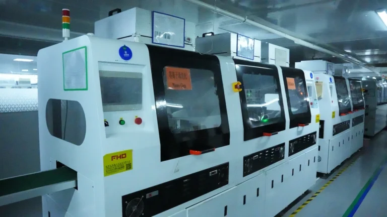
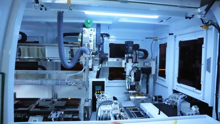
5.1 The Mainstream Process: Vacuum Thermal Evaporation
The dominant manufacturing method for OLED displays is vacuum thermal evaporation. The process involves:
- Depositing an ITO layer on a glass substrate to form the anode.
- Placing the substrate in a high-vacuum chamber.
- Sequentially evaporating the organic layers — hole transport layer, emissive layer, electron transport layer — and finally the metal cathode.
- Using a Fine Metal Mask (FMM) to define the pixel patterns during deposition.
This process is material-intensive — only about 30% of the evaporated material actually ends up on the substrate, with the rest being wasted.
5.2 The Emerging Alternative: Inkjet Printing (IJP)
Inkjet printing offers a compelling alternative. Instead of evaporating materials in a vacuum, a precision printer deposits OLED materials — including the RGB light-emitting materials — exactly where they are needed.
The advantages are significant:
- Material utilization reaches nearly 90%, compared to ~30% for evaporation.
- Lower production costs due to reduced waste.
- Suitability for large-area panels.
In 2025, TCL CSOT began mass-producing inkjet-printed OLEDs on its 5.5-Gen line and started constructing a $4.15 billion 8.6-Gen inkjet printing production line in Guangzhou. At SID Display Week 2025, the company showcased inkjet-printed OLED panels ranging from 6.5 inches to 65 inches — demonstrating the technology’s versatility across nearly every device category.
5.3 Encapsulation: The Achilles’ Heel
OLED materials are extremely sensitive to moisture and oxygen — exposure causes “dark spots” where pixels stop working. This is why OLEDs must be hermetically sealed immediately after fabrication.
Thin-film encapsulation (TFE) is the core technology ensuring the reliability of next-generation displays. Advanced encapsulation barriers now achieve water vapor transmission rates below 5 × 10⁻⁵ g/m²/day, enabling flexible and even stretchable OLED displays.
6. Types of OLEDs
6.1 By Driving Method
OLEDs are categorized by how they are addressed electronically:
- PMOLED (Passive-Matrix OLED) — Uses a simpler driver design without storage capacitors. PMOLEDs are cheaper to manufacture but limited in size and resolution — the largest PMOLEDs are only about 5 inches, with most being 1 to 3 inches. They are suitable for small displays like those in MP3 players and simple wearables.
- AMOLED (Active-Matrix OLED) — Each pixel is controlled by a thin-film transistor (TFT) that includes a storage capacitor. AMOLEDs consume less power, offer faster refresh rates, and can be built in large sizes with high resolutions. This is the technology used in virtually all modern smartphones, tablets, laptops, and TVs.
6.2 By Form Factor and Function
OLEDs can also be classified by their physical characteristics:
- Transparent OLEDs — can be embedded in windows or car windshields.
- Top-emitting OLEDs — emit light through the top surface, enabling higher aperture ratios.
- Flexible and Foldable OLEDs — enabled by OLEDs’ simple, thin construction. Samsung Display’s latest foldable OLED panels have passed 500,000-fold durability tests.
- White OLEDs (WOLEDs) — used in lighting applications and, with color filters, in TVs.
7. Advantages and Challenges
7.1 Core Advantages
OLEDs offer a compelling set of benefits over LCD technology:
- Superior image quality — perfect blacks, infinite contrast ratio, wider color gamut, and wider viewing angles.
- Ultra-thin and lightweight — panels less than 1 mm thick.
- Fast response times — OLEDs can switch on and off much faster than LCDs, eliminating motion blur.
- Lower power consumption — only lit pixels consume energy; in most use cases, OLEDs are more efficient than LCDs.
- Flexibility — the simple design enables flexible, foldable, rollable, and even stretchable displays.
7.2 Ongoing Challenges
Despite these advantages, OLEDs face several hurdles:
- Lifetime — OLED materials, particularly blue emitters, degrade over time. While lifetimes have improved dramatically, they still fall short of LCDs in some applications.
- Cost — OLEDs remain more expensive to manufacture than LCDs, though the price gap continues to narrow.
- Blue emitter stability — the efficiency and stability of blue OLED materials remain the primary bottleneck for the technology. LG Display’s planned introduction of blue PHOLED technology — announced for SID Display Week 2025 — represents a significant milestone toward addressing this challenge.
8. Conclusion: The Future of OLED
The journey of OLED from laboratory curiosity to commercial reality began with the seminal 1987 paper by Ching Tang and Steven Van Slyke at Eastman Kodak. Their heterostructure device produced measurable light emission at voltages below 10 V — a breakthrough that launched an entire industry.
Today, OLEDs are the dominant display technology in smartphones, with nearly a billion AMOLED screens produced annually. They are increasingly found in laptops, tablets, monitors, TVs, wearables, and AR/VR devices.
The future points toward even greater innovation:
- Flexible and foldable displays are already on the market and growing in popularity.
- Inkjet-printed OLEDs promise to lower costs and enable larger panels.
- Transparent and stretchable OLEDs open entirely new application domains — from car windshields to wearable e-tattoos.
- Blue PHOLED and TADF technologies continue to push efficiency and lifetime boundaries.
Will OLED completely replace LCD? The answer depends on continued progress in cost reduction, blue emitter stability, and large-area manufacturing. But one thing is certain: OLED has already transformed how we see the world through our screens — and the best is yet to come.